PCB Capability
| No | Things | Ability |
| one | PCB Layers | 2 ~ 15 layers |
| two | PCB Base Materials | FR4, High Tg FR4, Halogen Cost-free, Isola, Rogers, Aluminium |
| 3 | PCB Finished Board Thickness | .2mm ~ 7.0mm(8mil-276mil) |
| four | PCB Copper Thickness | one/3oz ~ 7oz |
| 5 | PCB Surface Finishing | HASL, Lead Free of charge HASL, Immersion tin, Immersion gold, Gold plating, Immersion silver, OSP, Carbon, and so forth. |
| six | PCB Max gold plating thickness | 50 microinch |
| 7 | PCB Min. Trace Width/Place | .075/.075mm(3/3mil) |
| eight | PCB Min. Finish Holes Dimension | .1mm(4mil) for laser holes .2mm(8mil) for mechanical holes |
| 9 | PCB Max.Finshed Measurement | 600mm x 900mm (23.6″ x 35.forty three”) |
| ten | PCB Hole Tolerance | PTH:±0.076mm(+/-3mil), NTPH:±0.05mm(+/-2mil) |
| 11 | PCB Soldermask Colour | Inexperienced, White, Black, Purple, Yellow, Blue, |
| twelve | PCB Silkscreen Color | White, Black, Yellow, Blue |
| 13 | PCB Impedance Control | +/-10% |
| fourteen | PCB Profiling Punching | Routing, V-Minimize, Chamfer |
| fifteen | PCB Special Holes | Blind/Buried holes, Countersunk holes |
| sixteen | PCB Reference YWIN | IPC-A-600H Class 2, Course three, TS16949 |
| seventeen | PCB Certificate | UL, ISO9001, ROHS, SGS |
| 18 | PCB Package | Vacuum & Carton |
PCBA Potential
| NO | Objects | Capacity |
| one | PCB Assembly Min. IC Pitch | .30mm(12mil) |
| 2 | PCB Assembly Foot Pin | SO, SOP, SOJ, TSOP, TSSOP, QFP, BGA and U-BGA |
| three | PCB Assembly Min. Chip Placement | 514 05 |
| 4 | PCB Assembly Max. PCB Dimension | 410mm x 600mm(16.two” x 23.six”) |
| 5 | PCB Assembly Min. PCB Thickness | .35mm(13.8mil) |
| six | PCB Assembly Maximum BGA Dimension | 74mm x 74mm(two.9″ x 2.9″) |
| seven | PCB Assembly BGA Ball Pitch | 1mm ~ 3mm(4mil ~ 12mil) |
| eight | PCB Assembly BGA Ball Diameter | .4mm ~ 1mm(16mil ~ 40mil) |
| 9 | PCB Assembly QFP Lead Pitch | .38mm ~ 2.54mm(15mil ~ 100mil) |
| ten | PCB Assembly Package | Anti-static Bubble Bag & Carton |
Company Details
Since the set up of Jiudu, the company has devoted to PCB and PCBA growth, continually growing the company’s components gear and enhancing its complex energy. The high quality principle of “continuous enhancement, pursuit of excellent high quality, comprehensive conference customer requirements” makes a broad consumer base and a good status in the industry. It is business relevant to double-sided PCB and large specific multi-sided board(300000 feet/thirty day period), SMT(8 line), DIP(4 line)computerized wave soldering, concluded solution assembly, and so on, can provide consumer with OEM and ODM a single-stop fast delivery support.
Factory Glance
Our Services
| Inquiry | 1. Please deliver the BOM record and PCB Gerber information to us for detail quotation |
| 2. If you require to design and style, make sure you supply us the schematic, features of product, dimension and so forth. Sample and Photo would be far better. | |
| Quotation | one. Engineer confirms PCB requirements and Purchasing section confirms parts. |
| two. Quotation will be provided within 3 working days. | |
| Payment | With regards to payment term: T/T, L/C, Western Union, Paypal |
| Sample generating | A handful of samples will be developed ahead of complete production all steps are strictly executed by business control and quality handle. |
| Mass Generation | Right after sample confirmed discussion about packing, shipping and delivery. Manufacturing division start off the buy plan. |
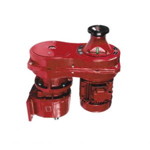
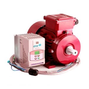
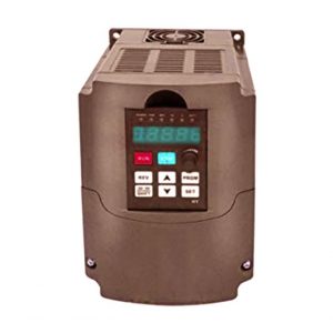
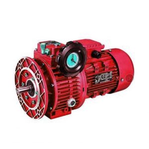
Our Gear
Packaging & Shipping
About packing
For PCB
For PCBA
Inner packing: Vacuum and Anti-static bubble bag.
Outer packing: 5-layer extremely hard Higher standard cartons box.
Delivery Details: Sample5-7 days, Mass: fifteen-25days
About delivery
FAQ
Q1: What data files do you use in PCB fabrication?
A1: Gerber, pcb. Automobile CAD
Q2: How do you make positive the quality?
A2: Our Merchandise is all 100% examined which includes Flying Probe Check (for sample), E-examination (mass) or AOI.
Q3: Can we pay a visit to your firm?
A3: Of program! Welcome to visit our business, JIUDU is positioned in Montreal YWIN Park, Quebec province, china.
Q4: What is the direct time?
This autumn: It requires 3-5 doing work days for sample, 7-ten working times for batch creation primarily based on documents and quantity.
Q5: Will you maintain our details and data files key?
A5: Positive! It is our fundamental basic principle to preserve enterprise tricks to defend our customers’ rights and behalf.
Q6. How to function with you?
A6: -E-mail and send out us the PCB Gerber file, BOM list
– We will provide reply affirmation in twelve hours and reply to the offer you within 3-five times.
– Waiting around for your company to verify the cost, order and payment method.
– We will commence the manufacturing.